Semi-Solid State Battery Thermal Interface Materials
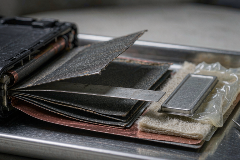
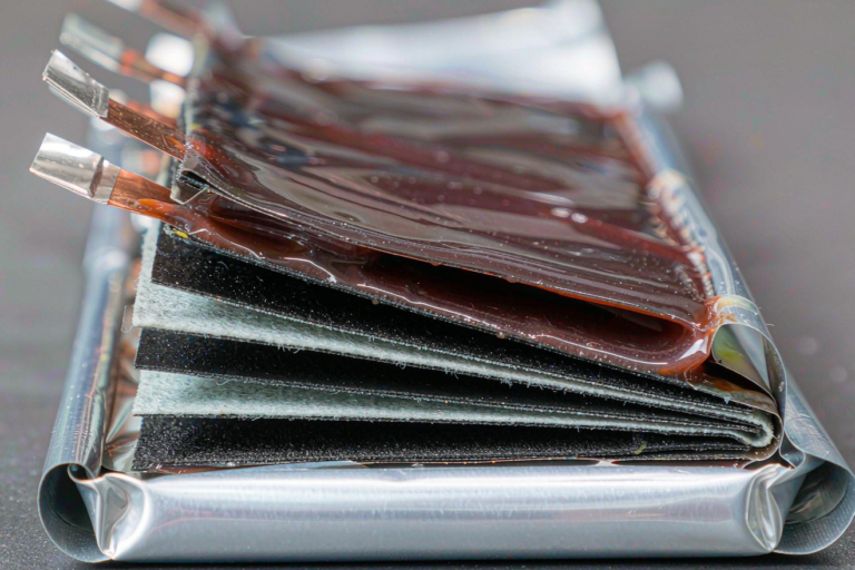
Karl Huang here, senior lithium battery engineer. When my team moved from conventional lithium battery packs to semi-solid state battery modules, the thermal stack looked familiar: cells, a cold plate, and a compliant layer between them. It was not familiar at all. Semi-solid cells want higher stack pressure, they breathe more across state of charge, and they tolerate a narrower temperature window than the prismatic cells I had built for a decade. The thermal interface material stopped being a gap filler and became a structural and reliability component. What follows is the selection and qualification process I now insist on before a single module gets bonded.

Where the Heat Actually Crosses a Semi-Solid Pack
Draw the heat path first. Energy leaves the electrode stack, crosses the cell can or pouch wall, crosses the thermal interface material, and enters the cold plate. Each step is a thermal resistance in series, and the largest one is rarely the one engineers argue about.
The resistances in series
Take a 300 cm2 cell face. An alumina-filled gap filler at 3.0 W/mK with a 250 micron bond line gives 0.83 K-cm2/W. The two contact interfaces add roughly 0.2 to 0.5 K-cm2/W each, depending on surface finish and pressure. That is the whole sandwich, under 2 K-cm2/W when it is assembled correctly.
Now put a 100 micron air void in it. Air conducts at 0.026 W/mK, so that same 100 microns becomes 38.5 K-cm2/W, about 40 times worse than the filled gap. A dispense pattern leaving 5 percent void area does not raise average resistance by 5 percent. Heat crowds around the void and the local spot runs far hotter than the average implies. Voids, not bulk conductivity, are what kill cells.
The same logic applies to the interfaces people forget: busbar to cold plate, MOSFET and gate driver boards, pre-charge resistor pads, fuse and contactor mounting faces. Those are small areas carrying real power, so a 1 K-cm2/W interface there deserves more attention than a 10 percent gain on a large cell pad.
Reading a Thermal Interface Material Datasheet
Bulk thermal conductivity in W/mK is the number printed largest and the least useful. It is measured on a slab by ISO 22007-2 or ASTM E1530, often at a thickness your assembly will never see. Design with thermal impedance instead: apparent thermal resistance measured by ASTM D5470 at a stated bond line thickness and a stated pressure.
Three numbers that change your design
- Impedance at your bond line and your pressure, not the vendor best case. Gap fillers improve 30 to 50 percent between 0.1 MPa and 1 MPa, so a value quoted at 1 MPa tells you nothing about a 0.2 MPa pack.
- Compression set after 1000 hours at 100 degrees Celsius. Anything above 20 percent means stack pressure decays and cell impedance creeps up with it.
- Dielectric strength and volume resistivity after aging, not just as molded. For an 800 V pack, keep at least 0.5 mm of dielectric material and verify 2.5 to 3 times the working voltage after the aging soak.
Ask for the impedance versus bond line curve as a graph. A single point hides whether the material is limited by bulk resistance or by contact resistance, and those two limits lead to opposite design fixes. Request the cure schedule, UL 94 rating, usable temperature range, and volatile content as well if the pack is sealed.
Filler Chemistry and What You Trade Away
Every thermally conductive compound is an insulating polymer loaded with filler until the particles touch. Percolation is the whole game, and it usually takes 50 to 70 percent filler by volume before the composite passes 3 W/mK. That loading is what makes the material viscous, dense, and stiff, which is exactly what you do not want in a gap that has to stay compliant for ten years.
- Alumina, roughly 30 W/mK, is the workhorse: cheap, electrically insulating, and it survives the loading without turning brittle.
- Zinc oxide, roughly 60 W/mK, buys a little more conductivity but adds density and cost.
- Boron nitride, about 300 W/mK in plane and only a few W/mK through plane. Good for spreading sideways, poor as a through gap filler unless the platelets are oriented.
- Aluminum nitride, roughly 170 W/mK, performs well until moisture reaches it; hydrolysis releases ammonia, which is unkind to everything else in a sealed enclosure.
- Graphite and graphene post the highest in-plane numbers and are electrically conductive. Next to live terminals that is a short circuit waiting to happen.
Silicone is the usual binder and it brings a specific hazard. Cyclic siloxanes volatilize, migrate, and under arcing decompose into insulating silicon dioxide. I have opened contactors whose contacts wore a fine white film that read open circuit. If your module contains relays or contactors, specify a low-volatile silicone with test data, or move to a polyurethane or olefin system, then verify contact resistance after the thermal aging soak.
Bond Line Thickness, Compression, and Stack Pressure
Bond line thickness is set by the mechanical design, not by the tube you dispense from. Two machined plates with 0.2 mm per metre flatness deviation across a 200 mm face can present a 0.4 mm gap difference corner to corner. Pads want 10 to 30 percent compression to wet out the surface. Dispensed gap fillers work from about 0.2 to 1.5 mm as cured.
Let the pad set the pressure, not the interface material
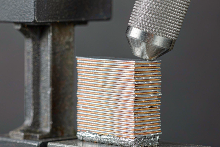
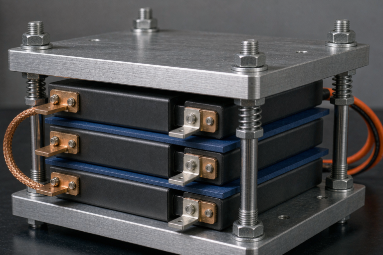
Semi-solid cells typically want 0.05 to 0.3 MPa of stack pressure, and some lithium metal designs push toward 1 MPa. Take 0.2 MPa over a 300 cm2 face: that is 6,000 newtons, about 610 kilograms of force, spread across a compliant layer. If the thermal interface material is the only thing resisting that load, it extrudes out of the gap and the cell loses both cooling and pressure.
Separate the jobs. Springs or a closed-cell silicone foam pad set the pressure; a pad delivering 0.05 to 0.25 MPa at 25 percent deflection is a reasonable starting point. The interface material only fills space and carries heat. Machining and mechanical stops control the gap. Never let one part do two jobs.
Then account for breathing. Graphite-based cells swing about 1 to 2 percent in thickness over state of charge. Silicon-blended anodes reach 4 to 8 percent. Semi-solid designs with lithium metal can move 5 to 15 percent, which on a 10 mm thick cell is up to 1.5 mm of cyclic travel pushing material in and out of the gap on every charge.
Failure Modes Across a Ten-Year Pack Life
- Pump-out. Greases are the worst offenders. Thermal cycling plus the coefficient of thermal expansion mismatch between an aluminium plate and a steel can squeezes material out of the interface. A 100 mm interface seeing a 60 K swing moves about 66 microns differentially, enough to pump a thin paste out over a few hundred cycles. The symptom is DCIR rising 5 to 15 percent with no capacity fade.
- Dry-out. Oil migrates out of a silicone pad and leaves a dry skeleton with two to four times the impedance. Bead density and oil bleed data are the predictors.
- Compression set. A cheap foam takes a permanent set after 1000 hours at 100 degrees Celsius, stack pressure falls, and cell impedance climbs even though nothing cracked.
- Void growth. Dispense voids start small and grow under thermal cycling. Target under 2 percent void area and inspect the first article by cross section.
One design decision deserves its own paragraph. Between a cell and a cold plate you want a conductor. Between neighbouring cells you often want a barrier. Aerogel and ceramic fiber paper run 0.02 to 0.05 W/mK and survive 800 to 1000 degrees Celsius, the opposite of what a thermal interface material does. Do not specify one material to do both jobs.
Qualification and In-Line Verification
My acceptance protocol is deliberately boring, and it has caught every bad batch so far.
- ASTM D5470 impedance at the production bond line and at 0.2 MPa, before and after aging.
- Aging matrix: 1000 hours at 85 degrees Celsius, 1000 hours at 85 degrees Celsius and 85 percent relative humidity, 1000 thermal cycles from minus 40 to 85 degrees Celsius with 30 minute dwells, and 500 pressure cycles between 0.05 and 0.3 MPa.
- Acceptance thresholds: impedance increase under 25 percent, no cracking or delamination, compression set under 20 percent, and at least 80 percent of original dielectric strength retained.
- Supporting tests: ASTM D575 compression deflection, ASTM D395 compression set, UL 94 V-0 rating, and module safety per IEC 62619 and UL 1973.
- Sealed enclosures: ASTM E595 outgassing, total mass loss under 1.0 percent and collected volatile condensable material under 0.1 percent.
On the line, meter the dispense by mass rather than by time, verify bead continuity with a 2D or 3D vision check, and cure a witness coupon every shift. Cut the coupon and measure the bond line at five points. Once the first article passes, repeat a thermal transient structure function test every 500 units; a rising interface resistance appears there long before a thermocouple notices.
Frequently Asked Questions
What makes a thermal interface material suitable for semi-solid state battery cells?
Look for low thermal impedance at your actual bond line and pressure, high dielectric strength after aging, and enough compliance to survive 5 to 15 percent cell breathing without pumping out. Compression set below 20 percent after 1000 hours at 100 degrees Celsius is the single best predictor of ten year stability.
How thick should thermal gap filler be in a battery module?
Most dispensed gap fillers cure between 0.2 and 1.5 mm, and pads usually sit between 0.5 and 3 mm at 10 to 30 percent compression. Choose the thickness from your tolerance stack, then confirm the material still meets the target impedance at that thickness and at your stack pressure.
Can I use thermal grease instead of a gap filler pad?
Only for a clamped interface with very flat surfaces and a small bond line, such as a busbar joint. Grease pumps out under thermal cycling and pressure cycling, and a semi-solid pack has both. For cell to cold plate interfaces I use a cured gap filler or a compression pad.
Does the thermal interface material affect UN 38.3 or IEC 62133 testing?
UN 38.3 covers transport and IEC 62133-2 applies to portable cells, so neither tests the interface material by name. Module and pack safety runs through IEC 62619 and UL 1973, where a material that fails, cracks, or burns can change temperature rise and thermal runaway propagation results.
How do I detect a thermal interface material that has pumped out?
Watch DCIR at a fixed temperature and state of charge. Pump-out shows as a gradual 5 to 15 percent DCIR rise with no capacity fade, plus a widening spread between hottest and coolest cells. Thermal transient structure function testing confirms the interface resistance increase before it becomes a field failure.
Is silicone safe near high voltage contactors?
Not always. Cyclic siloxanes outgas, migrate, and break down into insulating silicon dioxide under arcing, which raises contact resistance in relays and contactors. Use a low volatile silicone with documented ASTM E595 data, or specify a non-silicone system, and verify contact resistance after thermal aging.
Further Reading
References